|

Averatek Revolutionizes with New Chemistry that Allows Easy Soldering to Aluminum
By Tara Dunn, VP Marketing
Headquartered in Northern California, Averatek Corporation develops and licenses advanced manufacturing processes for numerous electronic products including very high density printed circuit boards (PCB), semiconductor packaging, and RF and millimeter wave passive components. Additionally, the company develops and sells key chemistries that enable these advanced manufacturing processes.
Averatek was founded by SRI International, a global contract research and development institution and a team of Silicon Valley entrepreneurs. SRI was part of Stanford University as the Stanford Research Institute from 1946 until 1970 when it became an independent non-profit contract research firm. Scientists at SRI invented and patented the technology that is at the heart of the Averatek process. SRI remains a major shareholder in Averatek.
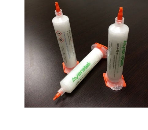
Averatek recently launched Mina™, a chemistry that offers exciting benefits over traditional methods of soldering to aluminum. Mina™ is a pretreatment for aluminum that allows soldering to aluminum as easily as soldering to copper. It can be printed onto aluminum pads using a stencil printer and cured at low temperatures. Mina™ can also be applied using other dispensing methods like syringe jetting. Aluminum costs significantly less than copper and can provide similarly low resistance at a greatly reduced weight.
Mina™ is an alternative method for advanced packaging and microelectronics that enables users to leverage the cost and weight benefits of aluminum. CEO Haris Basit added, “Mina truly is revolutionary. Until now, you could not easily solder to aluminum because of its natural oxide layer. Mina changes that, opening a new world of possibilities for users of low-cost circuit boards as well as high-power applications that benefit from low thermal resistance connections to aluminum heat sinks and chassis.”
Mina™ is unique because it solves a host of challenges. For example, typically there is an oxide present on all aluminum surfaces that inhibits solders from bonding with the core metal. To tackle this oxide, processes exist that involve a series of etchants and treatments that remove this oxide. This is commonly called the zincate process. Once the oxide is removed, the surface is plated with a noble metal finish like ENIG or ENEPIG to cover the surface and protect it from forming a new oxide layer. Mina, however, eliminates the need for all the wet chemistry and surface finishes. It is printed directly onto the aluminum pads using a stencil printer and cured at low temperatures. Cured Mina is non-conductive, which allows a uniform coating over the entire surface should the spacing between a component’s pads be too tight. After this, the boards can be stored since cured Mina remains stable, or the boards can go straight through the component assembly process, in which solder will be printed onto the pads, followed by component loading in the pick-and-place and then reflow. Mina activates during the reflow cycle and ensures a good solder joint to the core aluminum. Other than during the reflow cycle Mina remains completely inert.
Divyakant Kadiwala, VP of Manufacturing, added, “The solder selection depends on the substrate. A common use of aluminum is associated with aluminum on PET substrates or Al-PET substrate. PET cannot withstand high temperatures for an extended time, so low temperature solders become the favored option.”
Mina™ is a fit for numerous markets, especially those looking for lower cost PCBs:
• Automotive
• RFID
• Disposable electronics
• LED lighting panels, headlights and more
• Power electronics that directly connect high-power devices to aluminum heatsinks
• Markets that rely on mechanical bonding
“Mina™ has proven reliability in LED and automotive industries, as well as application in medical and mil/aero industries,” added Kadiwala. “Really Mina has application to any market that is looking to replace copper with aluminum. Aluminum is used in electronics for housings, chassis, heat sinks, low-cost circuit boards, traces and more.”
Additional benefits that Mina delivers include:
• Processing is more environmentally friendly and can be as short as a few seconds
• Produces superior solder joints
• Supports roll-to-roll manufacturing for mass production
• Replaces silver-based anisotropic conductive paste (ACP) with solder for economical manufacturing
• Reduces the carbon footprint through elimination of traditional wet chemistry and plating processes
To fully develop Mina, Averatek needed to partner with a best-fit electronics manufacturing services provider (EMS) to vet manufacturing processes for new technologies/products to bring to the market. After meeting more than a year ago at an industry networking event, Averatek partnered with Absolute EMS, Inc., a leading provider of turnkey and consignment manufacturing services. Absolute EMS assembles surface mount components onto polymer substrate with aluminum traces using Averatek’s Mina product. Additionally, the company performs developmental runs in its shop.
Doug Dow, Absolute EMS COO, said, “It truly is an honor to be in partnership with Averatek. Its mission is to create solutions that deliver ‘tomorrow’s technology,’ and this means that together we are working on things the industry has never seen before. The transparent polymer substrate can be a very thin piece of flexible PET with flexible aluminum traces where the components are placed with strategic accuracy. Averatek’s team of PhDs and scientists are working with Absolute EMS to continually push the boundaries of science and technology.”
Absolute EMS, located in the heart of Silicon Valley, is a leader in offering manufacturing services in a state-of-the-art, high-technology EMS facility. Founded in 1996, the company originally serviced the medical industry, thus its focus on controlled manufacturing that is scalable and repeatable. Since its inception, Absolute EMS has broadened its verticals to include medical, military, industrial, networking and engineering.
“It has been wonderful working closely with Absolute EMS on bringing this new capability to the market,” concluded Basit. “Absolute EMS combines the rigor and quality control of an established production facility with a flexibility and openness crucial to developing new products and processes. Finding one organization that encompasses both qualities has greatly accelerated our development cycle.”
To find out more about Averatek, contact Tara Dunn, VP Marketing, at 550 Nuttman St., Santa Clara, CA 95054; 408-496-1010; E-mail: info@averatek.com; Web site: www.averatekcorp.com.
Archives:
|
The latest news of people, products and production processes